


- Quadcept Support
- 15/08/17 14:50:40
Thank you for your inquiry. I'm extremely sorry for the delay in replying to you
because our office was closed from 13th to 16th August due to summer holidays.
In regard to the issue that you are inquring about, I would make a reply soon after
checking the content. So I would appreciate it if you would understand we have some time to answer it.
I'm sorry for troubling you but your cooperation would be highly appreciated.
- Quadcept Support
- 15/08/17 17:28:49
Thank you for your inquiry.
I apologize for the delay in replying to you.
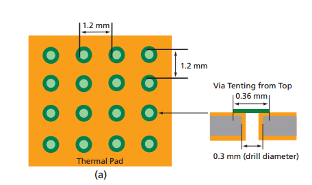
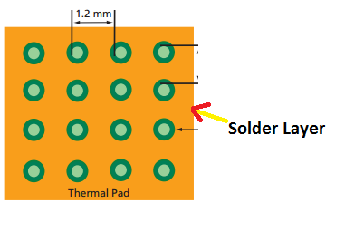
In regard to the issue you are inquiring about, an arbitrarily-shaped thermal pad is not
able to be created as a single pad stack, so please draw it on the PCB sheet directly or
create it in the footprint of a component.
In the case of creating on the PCB sheet directly,
it is possible by the following procedure.
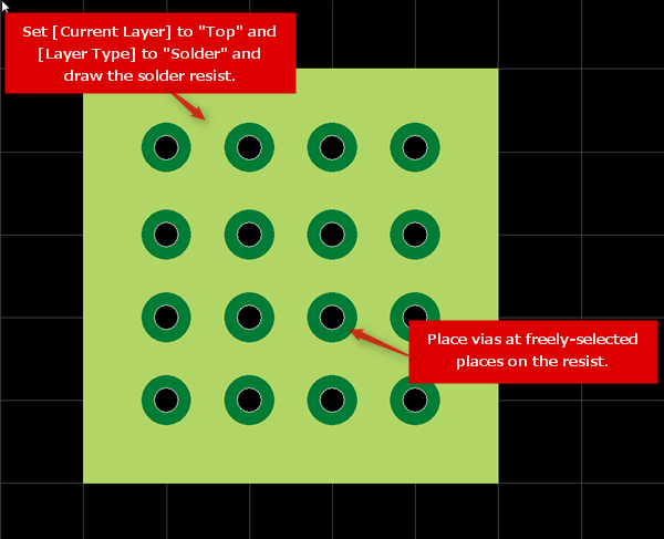
1) Set [Current Layer] to "Top" and [Layer Type] to "Solder".
2) Select 【Draw】 >> 【Filled Polygon】 or 【Filled Rectangle】 etc. and
draw the solder resist of a thermal pad using it on that layer.
3) Select any vias from the [Via] dialog(【Draw】 >> 【Via】) and place vias at freely-selected places on the resist.
When creating a thermal pad in the footprint of a component, it is necessary to be created
using the [Through] pad from the [Pad] dialog because vias cannot be used on the footprint sheet.
In the case of creating as a footprint, the procedure is as follows.
1) Set [Current Layer] to "Top" and [Layer Type] to "Solder".
2) Select 【Draw】 >> 【Filled Polygon】 or 【Filled Rectangle】 etc. and
draw the solder resist of a thermal pad using it on that layer.
3) Open the [Pad] dialog(【Draw】 >> 【Pad】) and create a [Through] pad.
4) Place the [Through] pads at freely-selected places on the resist.
* Please adjust the settings on the [Pad] dialog as needed.
* When it is created as a footprint, the number of pins existing in the component increases
because numbers will be assigned to all the placed [Through] pads, so please beware of it.
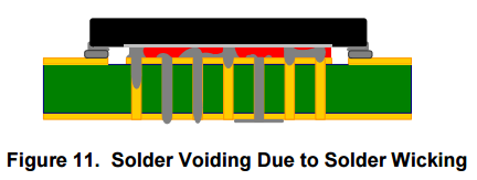
Finally, if the pad like the image you posted is created, I think DRC errors will occur but
please deal with the matter by ignoring them or changing them to [Approved].
I'm sorry for bothering you but please try above.
Thank you for your continuous support!